Thread
Much attention recently to dominance of Dutch giant ASML in advanced lithography + US efforts to restrict exports to China. But the real workhorse of industry is less advanced lithography, currently subject of trilateral negotiations on new controls. What is at stake? A thread.🧵
ASML’s cutting edge extreme ultraviolet (EUV) lithography enables the production of the most advanced semiconductors, used for smartphones, cutting edge CPUs and GPUs, and application specific integrated circuits used for autonomous driving and AI applications.
EUV systems are only used by a handle of firms globally: TSMC in Taiwan, Samsung in South Korea, and Intel in the US. SK Hynix and SMIC had planned to use EUV at China-based facilities, but were prevented by the multilateral Wassenaar Agreement, which controlled the gear in 2020. 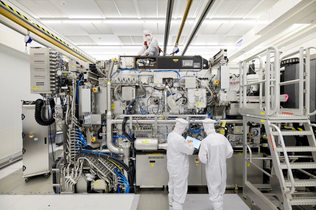

The US has controlled EUV technology for almost a decade. This is also a Wassenaar control, but there is no strict rule preventing the Netherlands from supplying Chinese firms with EUV. The Dutch government could issue licenses, for example. www.bis.doc.gov/index.php/documents/regulations-docs/2334-ccl3-8/file
Wassenaar Controls also extend to EUV masks and reticles in 2020. Hence all the EUV controls are also multilateral so far. www.federalregister.gov/documents/2020/10/05/2020-18334/implementation-of-certain-new-controls-on-eme...
So what about all the other firms manufacturing semiconductors? Many are using primarily what is called immersion lithography, under broad category of deep ultraviolet (DUV) lithography.
DUV, and specifically immersion DUV, is the critical technology at stake. Only ASML and Japan’s Nikon offer immersion lithography systems. Japan’s Canon also offers low-end dry DUV lithography equipment. But ASML dominates the higher end immersion lithography market. 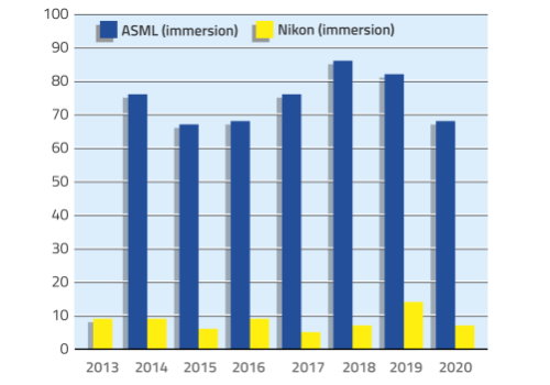

Hence the fact that the novel US controls released October 7 also capture DUV equipment is really important, because 1) they are unilateral, and 2) the US is trying to make them plurilateral, before making them multilateral, which has been the usual practice.
DUV controls were an implicit part of October 7 package, which includes end use controls on specific manufacturing nodes for logic/memory + new controls on specific equipment types under a new export administration regulation (EAR) category 3B090. www.federalregister.gov/documents/2022/10/13/2022-21658/implementation-of-additional-export-controls-...
The most expensive DUV immersion systems use 193 nm light from an ArF laser + project their patterns through a water layer between lens and wafer. They cost 60 million euros, less capable dry ArF systems are much cheaper, say 20 million euros, KrF machines cost 10 million euros.
Also critical to remember is that for advanced manufacturing, all these systems can be used on the stack of layers that make up a semiconductor. Some of the layers are more critical, some require EUV, for others DUV is fine. Thus, as EUV grows, DUV grows just as fast.
Thus DUV will remain highly relevant for semiconductor manufacturing, as EUV continues to be used @ cutting edge. ASML in 2021 sold total of 309 lithography systems, > previous year's 258 units, and ArF immersion systems (ArFi) accounted for 36% of sales, with 81 units shipped. 

ASML CFO: “That’s also why we still have extensive R&D programs for DUV...DUV will continue to represent a larger share of our business in future. Not only for memory but also applications/markets that use 90/ 65/45/28 nm. All are growing if you count number of wafers.”
Concern for US export control officials driving 7 October controls: technically, immersion DUV can be used for features sizes at 7 and even 5 nm, w/o EUV. Comes at cost of efficiency/commercial yield ..as more scale, whole cost structure more favorable to EUV on yield/cost.
A big issue for multinationals manufacturing memory in China is also transition from DUV to EUV. After the big 3 logic giants, memory manufacturers are now also looking at EUV. Samsung already uses EUV for DRAM production...TSMC also uses it for some DRAM for customers.
The decision to go from DUV to EUV is difficult: immersion systems are > half cost of EUV systems, and also more reliable and productive. ASML and Nikon are both offer high throughout speed in immersion: 275 wafers per hour. ASML’s new Twinscan NXT:2050i does 295 wafers per hour.
Negotiations now ongoing in The Hague and Tokyo almost certainly center on which DUV systems should be controlled, to which end users. It would not make sense to control non-immersion equipment, because Chinese supplier SMEE has lithography gear capable of 90 nm production. 

Both Japan + Netherlands will likely use list based controls, and not mirror end use and domestic persons controls incl in 7 October package. Status of lithography is critical, as it will determine what other tooling is likely to be affected as part of overall terms of agreement.
And, contrary to media reporting about an trilateral agreement, there does not appear to be a clear one hammered out yet, and the devil is way down in the details (that have not been released yet)...
...requiring understanding of different technologies, their tradeoffs/roadmaps, and supply chains. It appears so far to be a tall order for governments to negotiate without major industry input.